


Xiaomi—the Chinese brand best known internationally for its affordable smartphones and smart home gadgets—has quietly taken a bold leap into one of tech’s most competitive arenas: chip design. Its newly launched 3nm mobile SoC XRING O1 makes Xiaomi the fourth smartphone maker in the world to produce the 3nm SoC chip, after Apple, Samsung, and Huawei.
But Xiaomi's new chip puts the company at the center stage of the tech community: Is it truly “Made in China”? Can it be considered self-developed? And what does this move reveal about China’s broader ambitions in semiconductors and AI self-reliance amid rising geopolitical pressure?
Xiaomi’s re-entry into chipmaking—after a failed attempt nearly a decade ago—comes at a time when the global chip race is intensifying. To unpack what this means and why it matters, we’ve translated a highly respected Chinese analysis by Yuanchuan Tech review 远川科技评论 that addresses the five most frequently asked (and possibly misunderstood) questions about XRING O1. If you're tracking China’s tech trajectory, this is essential reading!
Xiaomi’s XRING O1: 5 controversies, unpacked
1. Is XRING O1 truly a Chinese chip?
This question could just as easily be reframed: Does Apple’s iconic A-series SoC qualify as an “American chip”?
As the current benchmark for many industry players, Apple’s debut A-series chip—the A4—had an underwhelming premiere 15 years ago.
During the hour-long keynote, the A4 appeared on screen for barely 20 seconds. Many in the industry mocked it as a “repackaged Samsung chip”—yet it was the result of Apple’s most ambitious internal effort at the time.
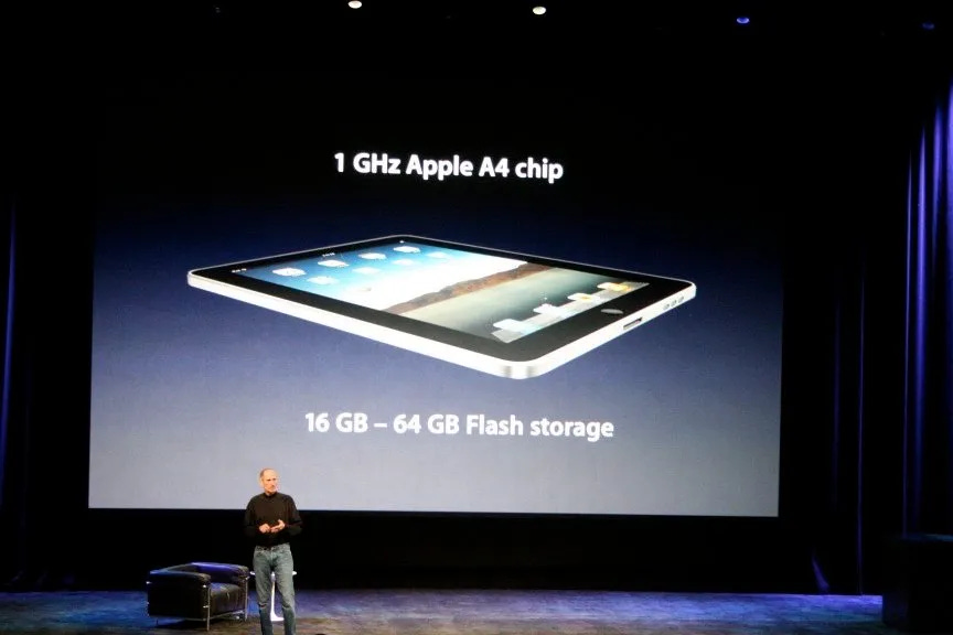
To bring the chip to life, Apple recruited legendary chip architect Jim Keller, IBM veteran Johny Srouji, and Daniel W. Dobberpuhl, who led the Alpha and StrongARM projects, via its acquisition of PA Semi.
Apple later acquired Intrinsity, a startup specializing in high-performance chip design. Samsung had used Intrinsity’s tech to build its own S5PC110 chip—powering the Galaxy S, a top rival to the iPhone. This explains why many saw the A4 and S5PC110 as “half-siblings.”
Apple’s heavy investment only brought it through the first phase of chipmaking: design.
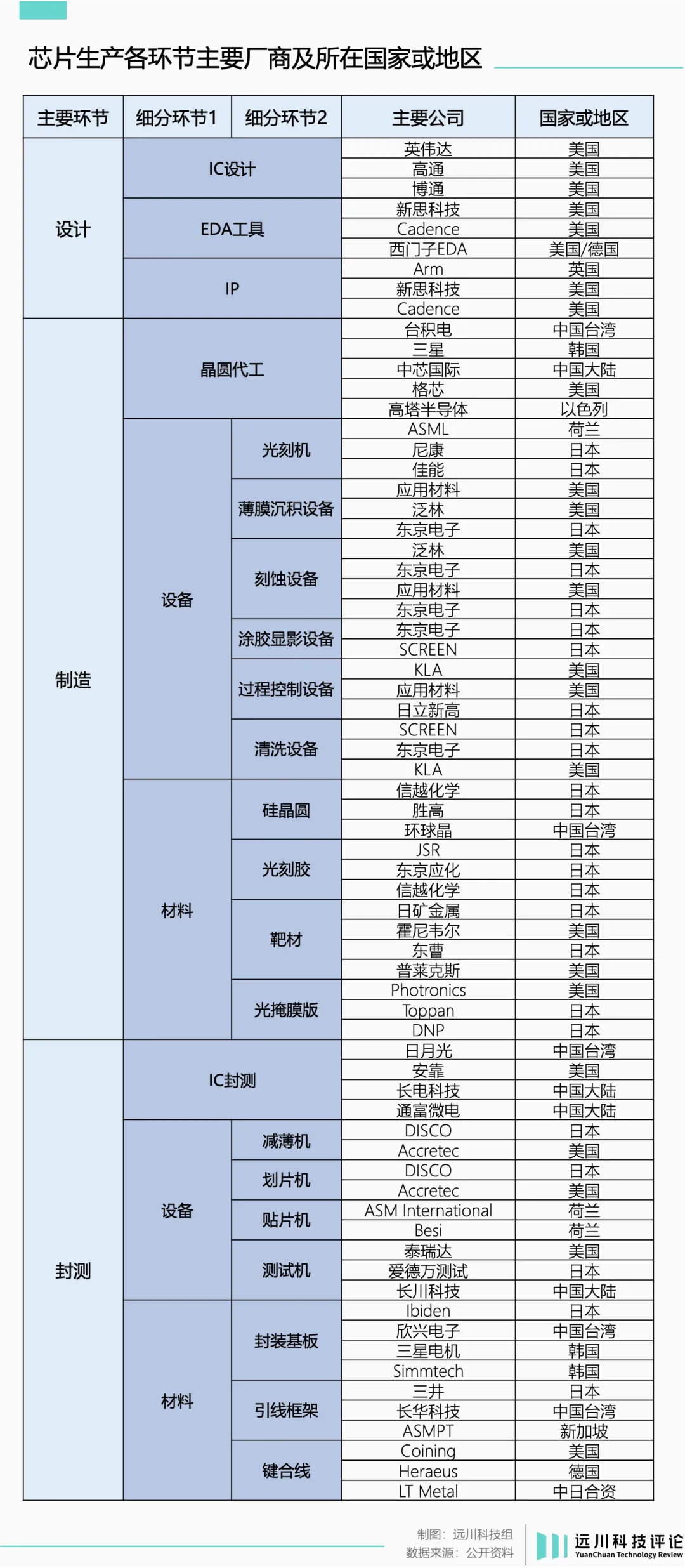
Semiconductor production typically spans three distinct stages: design, fabrication, and packaging/testing. Each is a standalone yet interconnected process, reflecting the deeply globalized and specialized nature of the industry.
Design work depends heavily on EDA tools from Synopsys, Cadence, and Siemens EDA (formerly Mentor Graphics), as well as IP cores from firms like ARM.
EDA tools and IP libraries are to chip engineers what Photoshop and stock images are to designers—transforming circuit layouts into intellectual work. Integrating tens of billions of transistors onto a fingernail-sized chip is impossible without them.
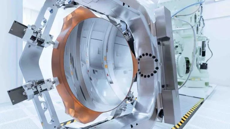
Once the design is complete, fabrication is handled by foundries like TSMC, Samsung, or GlobalFoundries. These firms rely on tools from ASML (lithography), Applied Materials (etching), Tokyo Electron (coating/developing), and KLA (inspection).
Each EUV lithography machine contains tens of thousands of components. Its most critical parts include Zeiss-made mirrors and a Cymer light source—producing high-intensity EUV light by firing 50,000 CO₂ laser pulses per second at liquid tin. This is the core technology the U.S. restricts for export.
During production, materials like photoresists are largely supplied by Japanese firms such as Shin-Etsu Chemical and Rohm.
Packaging and testing are dominated by Taiwan’s ASE Group, Amkor in the U.S., and Chinese firms like JCET and Tongfu Microelectronics—with many facilities located in Southeast Asia.
From design to activation in a device, a single chip’s journey spans more countries than most people do in a lifetime. Brands like Apple, Samsung, Huawei, and Xiaomi mainly handle the design phase.
Think of chips as Lego sets: design is the instruction manual. Japanese firms provide the plastic, TSMC or Samsung builds the parts, Southeast Asia assembles them—and they end up on store shelves.
If we define “domestic chips” as those whose IP is owned by a national company, then both Apple’s A-series and Xiaomi’s XRING O1 qualify.
But if the definition requires every stage of the chip’s production—and every tool and part—to originate from a single country, then no smartphone SoC in the world would qualify as “domestic.”
Not now, not before, and likely not ever.
2. Can XRING O1 be considered self-developed?
The XRING O1 was built using standard IP cores licensed from ARM—raising a common question: can it still be called “self-developed”?
In chip design, IP (Intellectual Property) refers to pre-designed circuit blocks that serve specific functions. A single SoC may be composed of dozens or even hundreds of such IP cores.
Designing a chip is much like assembling with Lego bricks, where the bricks are IP cores. Companies like Apple and Xiaomi use similar building blocks, but the architecture and integration define the end result—whether it’s a cottage or a castle.
Before ARM’s rise, most IP cores were developed in-house, requiring extensive verification. A simple digital IP block could cost $100,000 to $500,000 to validate, while a CPU core might demand over $2 million and take months or even years to fully test.
This high cost and long lead time crushed many design startups—and paved the way for ARM’s licensing model. ARM doesn’t design chips itself. Instead, it develops and licenses proven architectures and IP cores to design firms, who can either assemble chips entirely from ARM’s ready-made IP or integrate ARM IP with their own custom-designed blocks.
ARM’s licensing model—combined with its fair and accessible pricing—has dramatically reduced the design cost for companies seeking to build their own chips. This, in turn, lowered industry-wide barriers to entry. Since 2000, the number of chip design firms worldwide has grown from just over 200 to more than 1,000.
ARM also provides customized IP services—non-standard versions derived from its public cores that design firms can modify to meet their specific needs. While these customized cores come with higher licensing costs, longer verification timelines, and increased reliability risks, they also offer greater potential for product differentiation. In short, the opportunity comes with considerable risk.
Apple, Qualcomm, and Samsung have all ventured into custom IP—with very different outcomes.
Apple’s A-series adopted custom ARM cores starting with the third-generation A6, which introduced its proprietary Swift architecture—a critical milestone that brought its chip performance on par with industry leaders. By the time the A7 launched, Apple had overtaken its competitors in overall performance.
Qualcomm’s path has been more uneven. It began developing its custom Kryo core with the Snapdragon 820, but mounting R&D costs and downstream software compatibility issues forced it to pivot toward a hybrid model—combining ARM’s standard IP with selectively customized cores. It wasn’t until 2021, after acquiring Nuvia—a startup born out of Apple’s chip team—that Qualcomm began to realign its roadmap around Oryon, a fully custom core. Its efforts to reduce reliance on ARM only began to gain real traction from that point onward.
Samsung’s attempt was arguably the most ill-fated. Its first in-house Mongoose core debuted in the 2016 Exynos 8890, a direct challenge to Qualcomm’s Snapdragon 820. But the chip suffered from severe power inefficiencies, drawing heavy criticism for its thermal performance. The final iteration, the Exynos 990, faced open backlash from European consumers, many of whom publicly campaigned for Samsung to switch back to Snapdragon chips.
Using the same set of Lego bricks, one can create entirely different combinations, making the design process itself a legitimate form of self-developed innovation. Yet in the semiconductor industry, what ultimately defines a chip’s quality is its measurable technical specifications and the ability to achieve differentiated performance through close integration with software.
3. Why smartphone SoC R&D remains one of tech’s toughest challenges?
On this front, Xiaomi has stumbled before.
In October 2014, Xiaomi began developing its first smartphone SoC. The result—Pinecone Surge 1 (S1)—completed hardware design and underwent its first tape-out by July 2015. The first silicon samples were returned in September and successfully booted for the first time. In March 2017, the Surge S1 made its commercial debut inside the Xiaomi 5C.
Continue reading:
Q3 Why smartphone SoC R&D remains one of tech’s toughest challenges
Q4 What drives Xiaomi to develop its own SoC?
Q5 Is XRING O1 a success—or just a starting point?
You can also get free access by sharing us. For more timely discussions, consider joining our private Discord channel for paid readers.
